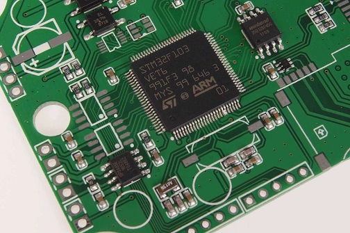
PCB stands for Printed Circuit Board. It is a crucial component in the field of electronics and is used to mechanically support and electrically connect electronic components using conductive pathways, tracks, or signal traces etched from copper sheets laminated onto a non-conductive substrate material.
Here are some key points about Printed Circuit Boards (PCBs):
-
Structure: PCBs are flat boards made from insulating materials such as fiberglass (FR-4) or composite epoxy. The non-conductive substrate provides mechanical support for electronic components and prevents electrical shorts.
-
Conductive Traces: Copper traces are etched onto the PCB to create pathways for electrical signals to flow between components. These traces can be single-layered (one side), double-layered (top and bottom), or multi-layered depending on the complexity of the circuit design.
-
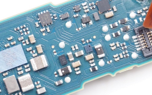
Components: Electronic components such as resistors, capacitors, integrated circuits, and connectors are mounted on the PCB using various methods like through-hole technology (THT) or surface-mount technology (SMT).
-
Functionality: PCBs act as the central nervous system of electronic devices, providing connectivity between components, enabling signal transmission, power distribution, and facilitating the overall functionality of the electronic system.
-
Types: There are various types of PCBs used in electronics, including:
- Single-layer PCBs: Contains copper traces on one side of the board.
- Double-layer PCBs: Contains copper traces on both the top and bottom sides.
- Multi-layer PCBs: Consist of several layers of conductive traces sandwiched between insulating layers. These are used in complex electronic devices to reduce size, improve performance, and enhance signal integrity.
-
Manufacturing: PCB manufacturing involves several steps, including design, substrate selection, copper etching, drilling, component placement, soldering, and testing. Advanced techniques such as automated assembly, surface mount technology, and inspection processes are used to ensure high-quality PCBs.
PCBs are fundamental components in electronic devices, ranging from simple gadgets like calculators and remote controls to complex systems like smartphones, computers, and medical equipment. Their design and quality significantly impact the performance, reliability, and cost-effectiveness of electronic products.
9 common sense of PCB inspection
PCB inspection is a critical aspect of the manufacturing process to ensure that the printed circuit boards meet quality standards and operate correctly. Here are nine common-sense practices for effective PCB inspection:
-
Well-Trained Personnel: Ensure that personnel involved in PCB inspection are well-trained and familiar with industry standards, inspection techniques, and common defects.
-
Visual Inspection Guidelines: Establish clear visual inspection guidelines to identify common defects such as solder bridges, misalignment, missing components, tombstoning, solder balls, and lifted pads.
-
Use Proper Lighting: Adequate lighting is crucial for visual inspections to detect defects accurately. Ensure that the inspection area is well-lit with appropriate lighting sources.
-
Magnification Tools: Provide magnification tools such as magnifying lamps, microscopes, or magnifying glasses for detailed inspection of fine-pitch components and solder joints.
-
Check Component Placement: Verify that components are placed correctly and oriented properly according to the assembly instructions and reference designators.
-
Solder Joint Quality: Inspect solder joints for proper wetting, fillet formation, and cleanliness to ensure solid electrical connections.
-
Check for Shorts and Opens: Use continuity testing procedures to check for shorts (unintended connections) and opens (broken connections) on the PCB.
-
Functional Testing: Conduct functional testing post-assembly to validate the operation and functionality of the PCB, ensuring that it meets the required performance specifications.
-
Documentation and Records: Maintain thorough documentation of inspection results, including defect identification, corrective actions taken, and records of inspected PCBs for traceability and quality control purposes.
By following these common-sense practices, manufacturers can enhance the quality assurance process, minimize defects, and ensure that PCBs meet the required standards for reliability, functionality, and performance.
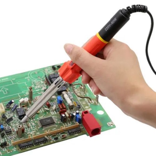
PCB board debugging method
Debugging PCBs (Printed Circuit Boards) is a crucial step in the electronics manufacturing process to identify and rectify faults or issues in the circuit design or components. Here are some common methods for debugging PCBs:
-
Visual Inspection:
- Perform a visual inspection of the PCB for any obvious defects like solder bridges, cold solder joints, misplaced components, or damaged traces.
-
Functional Testing:
- Power up the PCB and test its functionality using appropriate equipment. Verify that the board behaves as expected based on the design specifications.
- Use oscilloscopes, multimeters, logic analyzers, and other test equipment to analyze signals, voltages, and currents at different points on the PCB.
-
Signal Tracing:
- Trace the flow of signals through the PCB using a logic probe or oscilloscope to identify where a signal may be lost or corrupted.
- Verify that the signals are reaching the intended components and that there are no open or shorted connections.
-
Component Testing:
- Test individual components such as resistors, capacitors, diodes, transistors, and integrated circuits to ensure they are functioning correctly within the circuit.
- Use a component tester or multimeter to measure component values and characteristics.
-
Thermal Imaging:
- Use a thermal camera to detect hotspots on the PCB that may indicate components drawing excessive current or potential short circuits.
- Thermal imaging can help identify faulty components or areas of the PCB that are not functioning correctly.
-
Power Supply Analysis:
- Check the power supplies on the PCB to ensure that they are providing the correct voltages and currents to the components.
- Verify that the power distribution network is stable and not experiencing voltage drops or fluctuations.
-
Simulation Software:
- Utilize PCB design software with simulation capabilities to analyze the circuit operation virtually and identify potential design flaws or simulation mismatches.
- Simulate the circuit behavior under various conditions to pinpoint potential issues that may manifest during operation.
-
Reflow Soldering:
- If cold solder joints or insufficient soldering are suspected, consider reflow soldering specific areas of the PCB to ensure proper connections and soldering quality.
-
Incremental Testing:
- Break down the PCB testing into smaller sections or subsystems. Test each section individually to isolate the faulty area before testing the entire circuit.
-
Consultation and Collaboration:
- If you encounter complex issues that are challenging to resolve, don't hesitate to seek advice from experienced colleagues, online forums, or consult with experts in PCB design and debugging.
By using a combination of these methods, engineers and technicians can efficiently identify and resolve issues in PCBs, ensuring that the final product meets performance requirements and quality standards.
Finding the method of PCB board fault
When troubleshooting faults in a PCB (Printed Circuit Board), there are several methods you can employ to identify and rectify issues effectively:
-
Visual Inspection:
- Start with a detailed visual inspection of the PCB. Look for physical damage, burnt components, corrosion, solder bridges, missing components, or any other anomalies that could indicate a fault.
-
Continuity Testing:
- Use a multimeter in continuity mode to check for opens (broken connections) and shorts (unintended connections) on the board. Verify the continuity of traces, connections, and components.
-
Power Supply Analysis:
- Measure the voltages at various points on the PCB to ensure that the power supply is delivering the correct voltages to components. Check for fluctuations, noise, or irregularities in the power distribution.
-
Signal Tracing:
- Trace the flow of signals through the board using a logic probe, oscilloscope, or signal tracer. Identify where the signal is lost or distorted to locate the fault.
-
Thermal Imaging:
- Use a thermal camera to detect hotspots on the PCB. Hotspots could indicate components drawing excessive current, faulty components, or potential short circuits.
-
Functional Testing:
- Power up the PCB and systematically test the functionality of each component and section of the circuit. Verify that the PCB operates as expected based on the design specifications.
-
Component Testing:
- Test individual components such as resistors, capacitors, diodes, transistors, and integrated circuits to ensure they are functioning correctly within the circuit.
-
Simulation Software:
- If you have access to PCB design software with simulation capabilities, use it to simulate the circuit operation virtually. This can help identify potential design flaws or mismatches.
-
Reflow Soldering:
- If poor solder joints are suspected, consider reflow soldering specific areas of the PCB to ensure proper connections and soldering quality.
-
Sectional Testing:
- Divide the PCB into sections and test each section separately. This approach can help isolate the faulty area and streamline the troubleshooting process.
- Expert Consultation:
- If you encounter challenging issues, consider seeking advice from experienced colleagues, online communities, or professional technicians specializing in PCB fault identification and repair.
By combining these methods systematically, you can effectively locate faults in a PCB, expedite the troubleshooting process, and ensure the PCB operates correctly according to design specifications.